
At low frequencies, PCB substrate selection can feel straightforward. A large range of digital, power, control, and general-purpose electronics. For all of these, standard FR-4 works well.
About Things like thickness, copper weight, Tg, and cost. The designers don’t consider much until the frequency rises.
The laminate, because of its dielectric properties, can affect impedance and signal loss.
Read to learn more about how PCB material selection changes at higher frequencies.
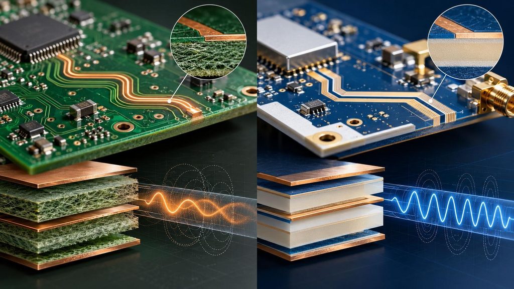
A short digital trace running at a few hundred megahertz may work great on ordinary FR-4. At higher frequencies or over longer transmission paths, losses accumulate, and small material variations become much more visible.
Two laminate properties get most of the attention:
Dielectric constant (Dk) affects impedance and propagation velocity. If the real Dk differs from the value used in the design model, the impedance and electrical length also shift.
Dissipation factor (Df) shows how much energy is lost in the dielectric. A lower Df often means lower dielectric loss, which gets important as frequency and transmission distance rise.
But Dk and Df are only part of the picture. At microwave and millimeter-wave frequencies, copper surface roughness, laminate thickness tolerance, moisture absorption, temperature stability, and surface finish can all influence performance.
That is why two laminates with the same published Dk values can work differently in the same RF circuit.
FR-4 stays attractive because it is inexpensive, widely available, mechanically familiar, and good with established PCB fabrication processes.
The issue is not that FR-4 cannot carry high-frequency signals.
The issue is that normal FR-4 was not developed mainly for tightly controlled microwave work. Its dielectric loss is higher than that of dedicated RF laminates, and its dielectric properties may change more with resin content, glass weave, frequency, temperature, and material construction.
For short transmission paths, the resulting loss may still be good. For a long RF feed, filter, antenna network, high-speed serial channel, or phase-sensitive circuit, the same loss and variation may get large.
This is why material selection should not be based on frequency alone.
A 3 GHz signal traveling a few millimeters on a board has very different needs from a 3 GHz signal traveling 200 mm through a tightly controlled RF network.
Materials such as Rogers RO4003C and RO4350B are often used when a design needs better RF performance without moving completely away from conventional PCB fabrication methods.
RO4003C, for example, has a typical Dk of 3.38 ± 0.05 and a dissipation factor of 0.0027 at 10 GHz. RO4350B has a Dk of 3.48 ± 0.05 and similarly targets RF and microwave applications. The RO4000 family is made to stay compatible with many standard FR-4 fabrication processes, which is one reason it comes up a lot in commercial RF hardware.
For more demanding microwave and millimeter-wave applications, PTFE-based materials such as RO3003 or RT/duroid 5880 give even lower dielectric loss.
RO3003 has a Dk of about 3.00 ± 0.04 and a dissipation factor of 0.0013 at 10 GHz. Rogers also offers RO3003G2 specifically for applications such as 77/79 GHz automotive radar, where very-low-profile copper and tighter electrical consistency get more important.
RT/duroid 5880 moves even further in low-loss RF performance, with a Dk of approximately 2.20 ± 0.02 and Df of 0.0009 at 10 GHz.
These numbers are useful, but they should not be looked at as a simple ranking in which the material with the lowest Df is automatically the best choice.
A lower-loss laminate may cost more, need different handling, show mechanical considerations, or give more performance than the application even needs.
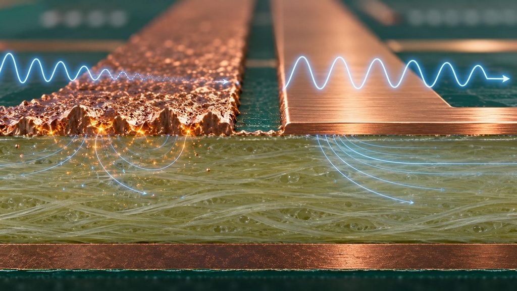
At low frequencies, engineers often focus mainly on the dielectric material. At microwave and especially millimeter-wave frequencies, that is not enough.
Current does not distribute uniformly in the full thickness of a copper conductor as frequency rises. The good current-carrying region moves toward the conductor surface because of the skin effect.
Once the skin depth gets comparable to the scale of the copper surface roughness, the electrical path is no longer well represented by a perfectly smooth conductor.
Rougher copper increases conductor loss and can also affect phase behavior. Rogers notes that copper roughness at the copper-to-substrate interface gets increasingly influential as frequency rises, mainly when the skin depth gets close to or falls below the roughness of the copper surface.
This is one reason low-profile, very-low-profile, or rolled copper is often thought of in high-frequency boards.
The effect gets visible at millimeter-wave frequencies. In Rogers testing at 77 GHz, circuits using smoother rolled copper showed lower conductor loss than otherwise similar circuits using rougher electrodeposited copper.
At that point, specifying only the laminate name is no longer enough. Copper type and roughness need to be part of the material definition.
Surface finish is another choice that gets more important as frequency rises.
For many conventional PCBs, ENIG is picked mainly because of solderability, storage life, and assembly needs. In an RF transmission path, however, the nickel layer beneath the gold has much lower conductivity than copper.
At sufficiently high frequencies, this can increase conductor loss.
Rogers specifically finds conductor finish as a contributor to microwave and millimeter-wave loss and notes that ENIG can cause higher loss than bare copper because of the conductivity difference between nickel and copper.
This does not mean ENIG should never be used on RF boards. It means the finish has to be thought of as part of the RF structure and not as a decision made only at the assembly stage.
For some designs, the RF transmission area and the component-assembly area may even justify different treatment.
A datasheet may list a Dk such as 3.0, 3.38, or 3.48, but the nominal value is only one part of the decision.
What matters just as much is how consistently that value is kept.
Variations in dielectric thickness and Dk change characteristic impedance. Changes in Dk with temperature also change electrical length and phase.
For many digital designs, the resulting difference may be insignificant. In filters, phased arrays, matching networks, radar circuits, and other phase-sensitive RF structures, it can directly shift circuit behavior.
This gets important in millimeter-wave systems, where wavelengths are short enough that relatively small physical and material variations represent a larger fraction of a wavelength.
Rogers thus finds Dk variation, thickness control, copper roughness, and temperature behavior as increasingly important material considerations in millimeter-wave PCB designs.
The useful implication is simple: high-frequency material selection is not only about picking a lower Dk. It is about picking a predictable Dk.
It is tempting to create a rule such as:
“Use FR-4 below 1 GHz, RO4350B up to 10 GHz, and PTFE above that.”
That may be convenient, but it is not a good engineering rule.
Material needs depend on the complete interconnect.
A low-loss material may be useless for a very short RF connection, and a long channel may justify better material at a considerably lower frequency.
The target should thus be electrical performance, not a material pick from frequency alone.
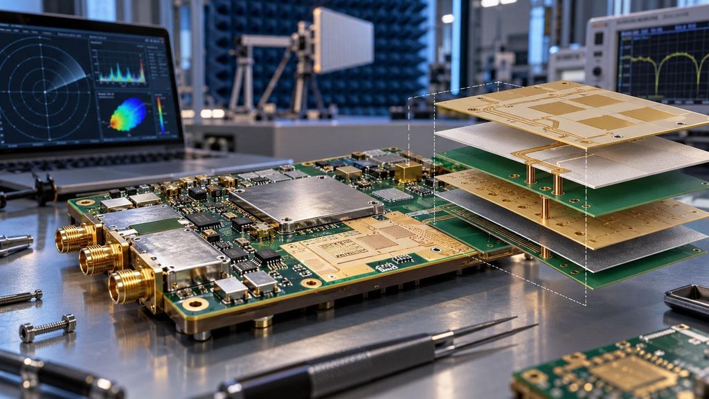
High-frequency material selection also does not have to be an all-or-nothing decision.
Many practical products have only a limited RF section. The rest of the board may have power conversion, microcontrollers, memory, interfaces, and other circuitry that works perfectly well with conventional FR-4.
In those cases, a hybrid stack-up can place a low-loss RF laminate only where the high-frequency circuitry needs it, while retaining FR-4 in other layers.
This way can lower material cost, but it introduces extra manufacturing considerations. The fabricator has to manage changes in material behavior, bonding systems, layer registration, drilling, plating, and final board thickness.
The stack-up thus needs to be checked as a manufacturing structure, not treating each laminate as an independent layer.
At higher frequencies, the electrical model and the fabrication process get increasingly difficult to separate.
A designer may measure the correct impedance using a published Dk, but the finished result still depends on real dielectric thickness, copper thickness, etching behavior, copper profile, and the material data used by the PCB manufacturer.
This is why high-frequency projects benefit from defining the stack-up before the layout is finalized.
The PCB manufacturer can confirm available laminate constructions, copper types, finished thickness tolerances, impedance capability, and whether the proposed hybrid material combination is feasible to be made repeatedly.
For ordinary boards, material selection may start with a laminate name.
For microwave and millimeter-wave boards, it increasingly becomes a controlled combination of dielectric material, copper, stack-up, geometry, fabrication process, and real operating conditions.
That is the real change as frequency rises.
Ans: PTFE-based and ceramic-filled high-frequency PCB materials are preferred for low signal loss and stable performance.
Ans: FR4 material works for lower frequencies but may cause signal loss at higher speeds.
Ans:CTE affects thermal reliability and prevents stress in multi-layer PCB material designs.
